1
00:00:00,100 --> 00:00:04,366
In this lesson, we're going to talk about the chip location recognition
2
00:00:05,533 --> 00:00:08,366
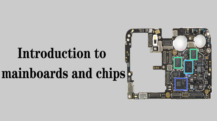
What we see now is the component map of the mainboard
3
00:00:10,133 --> 00:00:14,833
The component map of the mainboard is actually the identification or description
4
00:00:14,833 --> 00:00:16,566
of the main chips in the mainboard
5
00:00:21,200 --> 00:00:23,033
For example, in this mainboard,
6
00:00:23,266 --> 00:00:26,466
here is the Snapdragon 845 CPU
7
00:00:26,866 --> 00:00:28,900
Here is Samsung's font library,
8
00:00:29,066 --> 00:00:32,400
and these positions show the chips, audio chip,
9
00:00:32,400 --> 00:00:33,866
gravity sensor chip,
10
00:00:34,166 --> 00:00:36,833
fast charging chip, audio power amplifier,
11
00:00:37,100 --> 00:00:39,433
RF power amplifier, etc.
12
00:00:39,766 --> 00:00:42,466
Ok, let's talk about these chips separately
13
00:00:43,033 --> 00:00:44,766
Let's take a look at the CPU
14
00:00:44,966 --> 00:00:47,400
The CPU is the central processing unit
15
00:00:47,933 --> 00:00:52,100
The most important thing in a smart phone with good performance is the CPU
16
00:00:52,966 --> 00:00:55,866
It is the control center system of the mobile phone
17
00:00:55,866 --> 00:00:58,100
and the control center of the logic part
18
00:01:01,200 --> 00:01:02,733
Here is the CPU
19
00:01:02,966 --> 00:01:07,833
The picture on the right is the CPU of Qualcomm SM6150
20
00:01:09,033 --> 00:01:15,633
At present, the mainstream chip manufacturers for smartphones are those shown in the picture on the right
21
00:01:16,233 --> 00:01:20,533
Qualcomm, MediaTek, Hisilicon and Samsung
22
00:01:20,733 --> 00:01:21,666
Let's take a look
23
00:01:22,000 --> 00:01:22,866
Qualcomm
24
00:01:22,900 --> 00:01:25,966
The first row is the branding of Qualcomm processors
25
00:01:26,500 --> 00:01:30,000
Second row, SDM670 is the model
26
00:01:31,066 --> 00:01:32,066
MTK
27
00:01:32,233 --> 00:01:34,266
The first row is MediaTek logo
28
00:01:34,466 --> 00:01:39,200
The second row, the string begins with MT is the model of this CPU
29
00:01:41,200 --> 00:01:42,100
Hisilicon
30
00:01:42,433 --> 00:01:45,200
Hisilicon's CPU starts with Hi
31
00:01:46,500 --> 00:01:49,733
Hi6280 is the model of this CPU
32
00:01:52,366 --> 00:01:53,500
Samsung
33
00:01:53,766 --> 00:01:55,733
This is the Samsung's logo,
34
00:01:55,966 --> 00:01:59,000
980 refers to the model of this CPU
35
00:02:01,300 --> 00:02:04,066
Ok, let's take a look at the structure of the CPU
36
00:02:05,566 --> 00:02:08,200
The current CPU adopts double-layer welding,
37
00:02:08,900 --> 00:02:10,800
and the welding method is double-layer
38
00:02:11,366 --> 00:02:13,266
For example, in the picture on the right,
39
00:02:13,766 --> 00:02:15,166
it looks like a hamburger
40
00:02:21,000 --> 00:02:24,466
The top of the double-layer CPU is the temporary storage
41
00:02:25,966 --> 00:02:30,000
The codes engraved on its surface are the temporary storage models
42
00:02:30,766 --> 00:02:35,200
Only when the temporary storage is removed can we see the CPU model
43
00:02:36,300 --> 00:02:38,600
This structure of upper and lower layers
44
00:02:39,000 --> 00:02:43,033
we call it PoP structure, package stacking technology
45
00:02:43,833 --> 00:02:47,033
Laminate, stack up, that's what it means
46
00:02:48,000 --> 00:02:49,900
Well, this picture shows the CPU
47
00:02:49,900 --> 00:02:52,666
after removing the upper temporary memory chip
48
00:02:58,733 --> 00:03:00,700
This is the back of the CPU,
49
00:03:04,166 --> 00:03:07,500
SM8150 is the model of this CPU
50
00:03:11,166 --> 00:03:13,700
OK, that's it for the lesson of the CPU


