1
00:00:00,166 --> 00:00:04,266
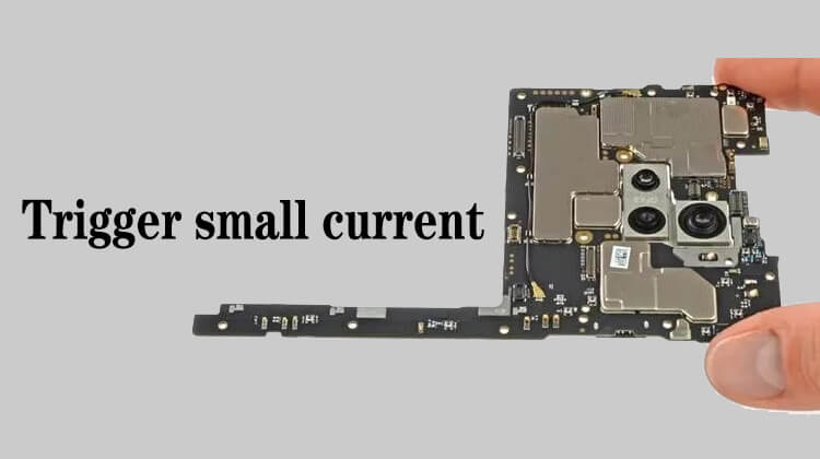
In this lesson we talk about the trigger small current related circuits
2
00:00:04,566 --> 00:00:07,000
Let's take a look at the startup workflow
3
00:00:08,700 --> 00:00:11,333
First of all, in the battery circuit,
4
00:00:11,700 --> 00:00:16,100
a battery positive pole comes out of the battery holder to the charging chip
5
00:00:18,200 --> 00:00:21,133
The MOS tube in the charging chip is turned on,
6
00:00:21,366 --> 00:00:26,700
VPH_PWR or VBT_SYS is generated
7
00:00:28,866 --> 00:00:32,200
This main power supply is transmitted to the power supply chip
8
00:00:32,466 --> 00:00:35,633
After the power supply chip receives this power supply,
9
00:00:36,100 --> 00:00:38,900
the clock circuit composed of the crystal oscillator
10
00:00:39,200 --> 00:00:42,400
and the power supply chip starts to work in standby
11
00:00:43,266 --> 00:00:45,100
After the power supply works,
12
00:00:45,166 --> 00:00:49,400
gives a voltage of 1.8 V to the power-on signal line
13
00:00:50,366 --> 00:00:54,133
The power-on signal line is the line connecting the power-on button
14
00:00:56,366 --> 00:00:57,866
We press the power button,
15
00:00:57,866 --> 00:01:02,100
that is, the signal of the power button is artificially grounded
16
00:01:04,600 --> 00:01:07,533
Pull down the voltage for more than 5 seconds,
17
00:01:08,700 --> 00:01:12,800
that is, press and hold the power button for more than 5 seconds
18
00:01:12,933 --> 00:01:16,666
At this time, the power chip will output power to the hard disk,
19
00:01:16,700 --> 00:01:20,100
CPU, baseband, and temporary storage
20
00:01:23,533 --> 00:01:25,566
After the power supply is output,
21
00:01:26,000 --> 00:01:28,933
the power supply will give a clock signal to the CPU,
22
00:01:29,033 --> 00:01:31,933
and the CPU will give a clock signal to the hard disk
23
00:01:34,400 --> 00:01:37,466
Clock signal abbreviated as CLK
24
00:01:37,666 --> 00:01:40,633
Then, the power goes to reset the CPU,
25
00:01:40,800 --> 00:01:42,766
and the CPU goes to reset the hard disk
26
00:01:43,933 --> 00:01:45,866
After the hard disk is reset,
27
00:01:46,733 --> 00:01:53,266
the CPU reads the boot program in the hard disk through the RX and TX communication protocol lines,
28
00:01:53,666 --> 00:01:57,166
and then performs a self-test on the CPU itself,
29
00:01:57,300 --> 00:02:00,033
the temporary storage, and the hard disk
30
00:02:01,733 --> 00:02:04,200
After the self-test is no problem,
31
00:02:04,400 --> 00:02:06,166
continue to load the system,
32
00:02:06,333 --> 00:02:12,433
and feed back and output a hold signal PS_HOLD to the power supply,
33
00:02:12,600 --> 00:02:15,266
and the power supply continues to output power
34
00:02:15,933 --> 00:02:18,666
Well, this is the boot process of a mobile phone
35
00:02:20,466 --> 00:02:22,366
Ok, that's it for this lesson


