1
00:00:00,333 --> 00:00:04,700
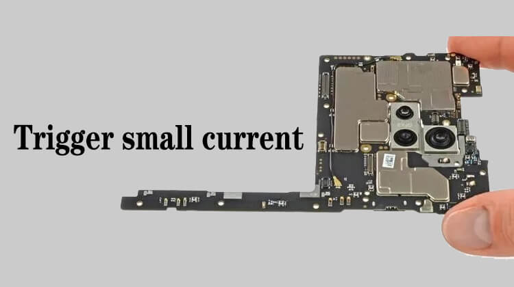
In this lesson, we talk about the circuits related to the trigger small current
2
00:00:08,100 --> 00:00:11,566
In the previous lesson we learned about the boot process
3
00:00:13,366 --> 00:00:15,933
Now let's take a look at what these terms mean
4
00:00:19,300 --> 00:00:22,400
VBAT refers to the positive pole of the battery,
5
00:00:23,933 --> 00:00:27,566
the negative pole is usually not shown on the block diagram
6
00:00:34,866 --> 00:00:38,233
Each chip has a ground wire, which is the negative pole
7
00:00:40,166 --> 00:00:42,800
The power chip, crystal oscillator,
8
00:00:43,066 --> 00:00:47,700
hard disk on the boot base, CPU, temporary storage,
9
00:00:48,200 --> 00:00:50,466
and other chips all have ground wires,
10
00:00:50,766 --> 00:00:53,133
but they are not marked in the block diagram
11
00:00:54,066 --> 00:00:56,666
Let's take a look at what these terms mean
12
00:00:57,866 --> 00:01:01,600
The MOS tube on this charging chip only acts as a switch,
13
00:01:02,666 --> 00:01:05,066
here is generally a PMOS tube,
14
00:01:05,500 --> 00:01:09,566
which is a P-channel MOS tube, which is used as a switch
15
00:01:10,766 --> 00:01:14,033
VPH_PWR is the main power supply
16
00:01:16,200 --> 00:01:21,000
This is a crystal oscillator with a frequency of 38.4MHz
17
00:01:21,566 --> 00:01:23,033
This is the power chip
18
00:01:23,633 --> 00:01:26,366
PWRON is the power-on signal
19
00:01:27,733 --> 00:01:32,166
What about KYPD_PWR? It is also a boot signal
20
00:01:33,133 --> 00:01:37,200
Xiaomi's boot signal is called PHONE_ON_N
21
00:01:47,400 --> 00:01:52,733
There are some other power-on signals are called KEYPD_PWR
22
00:01:53,366 --> 00:01:57,366
The power-on signal line has a variety of English references,
23
00:01:58,566 --> 00:02:00,166
This is the power button
24
00:02:00,666 --> 00:02:03,500
Where is the power button? It's on a seat,
25
00:02:04,333 --> 00:02:07,033
generally leading to a seat or a shrapnel
26
00:02:08,433 --> 00:02:12,333
Usually the socket it is attached to is called a boot socket
27
00:02:16,666 --> 00:02:18,133
This is a power supply,
28
00:02:18,466 --> 00:02:23,166
the power supply output to the power supply is not marked with its exact code
29
00:02:23,566 --> 00:02:28,733
In the drawing, the power supply starts with VREG or VOUT,
30
00:02:29,400 --> 00:02:33,500
or the chip pin output is VDD, VCC,
31
00:02:33,633 --> 00:02:36,600
generally the power supply starts with the letter V
32
00:02:42,900 --> 00:02:48,033
In the drawing, its expression may be VREG_UFS_3P0,
33
00:02:48,400 --> 00:02:52,300
and 3P0 represents the power supply of 3V
34
00:02:59,866 --> 00:03:02,233
There are a lot of power supply codes,
35
00:03:02,433 --> 00:03:05,266
because there are many brands of Android phones
36
00:03:05,500 --> 00:03:09,166
For example, VBUCK is also a common power supply
37
00:03:09,733 --> 00:03:12,733
These terms in the drawings all indicate power supply
38
00:03:14,133 --> 00:03:17,700
The CPU power supply is abbreviated as CORE,
39
00:03:18,033 --> 00:03:20,666
which refers to the power supply of the CPU core
40
00:03:20,866 --> 00:03:23,566
Of course, there are many ways for its power supply,
41
00:03:23,800 --> 00:03:26,800
including GPU, modem power supply
42
00:03:27,200 --> 00:03:29,366
This is just a rough reference
43
00:03:30,300 --> 00:03:35,233
In fact, there are as many as 20 to 30 power supplies for Android phones
44
00:03:35,500 --> 00:03:38,066
There is no way to label them one by one
45
00:03:39,300 --> 00:03:41,733
All we need to know is that on Android,
46
00:03:42,166 --> 00:03:45,666
there are about 20 to 30 power lines for the CPU,
47
00:03:45,900 --> 00:03:47,933
for the memory, for the hard drive
48
00:03:48,400 --> 00:03:50,333
CLK is the clock signal
49
00:03:53,300 --> 00:03:55,066
This is the reset signal
50
00:03:55,766 --> 00:03:57,500
This is a hold signal
51
00:04:00,400 --> 00:04:06,633
Similarly, this one is reset, sometimes abbreviated as RST
52
00:04:07,766 --> 00:04:10,433
This is CLK, the clock signal
53
00:04:12,800 --> 00:04:15,966
RX is receive, TX is transmit
54
00:04:16,933 --> 00:04:20,666
Here is a whole process of trigger small current at startup
55
00:04:21,833 --> 00:04:23,833
Okay, that's it for this lesson


